- Posts: 77
- Thank you received: 31
KiCad Schematics pedalSHIELD.
10 years 4 months ago - 9 years 6 months ago #24
by JR
keep it simple
KiCad Schematics pedalSHIELD. was created by JR
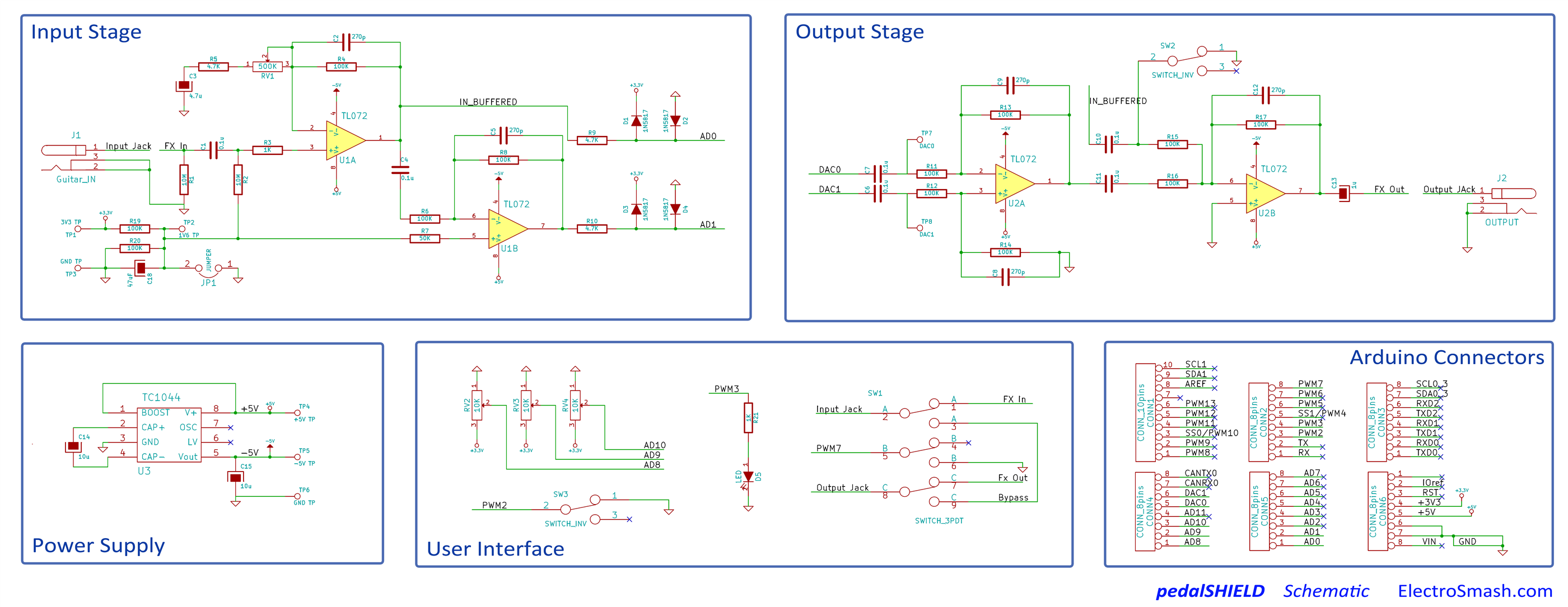
pedalSHIELD was developed using KiCAD.
KiCad is an EDA software tool for the creation of professional schematics and PCBs. KiCad runs on Windows, Linux and Apple OS X and is released under the open-source GNU GPL v2 free of charge.
The schematic files are public an open:
Full size pedalSHIELD schematic image link

KiCad is an EDA software tool for the creation of professional schematics and PCBs. KiCad runs on Windows, Linux and Apple OS X and is released under the open-source GNU GPL v2 free of charge.
The schematic files are public an open:
Full size pedalSHIELD schematic image link
keep it simple
Last edit: 9 years 6 months ago by JR.
Please Log in to join the conversation.
10 years 3 months ago #69
by wose
Replied by wose on topic KiCad Schematics pedalSHIELD.
Hi,
thanks for the pedalSHIELD. I'm in the process of extending it. I noticed that the schematics differ from the screenshot and the BOM you made public.
In the KiCad files are 2 more caps (C16,C17 100n) between +5 and GND, -5 and GND. The values of C2, C5, C8, C9 and C12 are 47p, the screenshot and the BOM lists these as 270p.
Can you give me a hint which revision is newer and why you made these changes.
Under wich license did you release the schematics? Am I allowed to modify and republish them?
Thanks again.
The following user(s) said Thank You: JR
Please Log in to join the conversation.
10 years 3 months ago - 10 years 3 months ago #70
by JR
")
keep it simple
Replied by JR on topic KiCad Schematics pedalSHIELD.
Yes, these 2 caps were place for super-filtering in the power supply but after tests I did not find any difference between placing them or not. The power lines are clean. So the footprints are in the PCB ( bottom left ) but they are not included in the BOM.In the KiCad files are 2 more caps (C16,C17 100n) between +5 and GND, -5 and GND.
The right value is 270pF, thanks for spotting that. I have updated the KiCad native files. I did several tests for filtering harsh high-freqs, I started using 47pF that is why that value was there. 270pF is a nice value, however there is not a big audible difference if you place 47pF.The values of C2, C5, C8, C9 and C12 are 47p, the screenshot and the BOM lists these as 270p.
Everything published in electrosmash.com (including these schematics) are under Creative Commons Attribution 3.0 , the less restrictive I have found. You're of course allowed to modify and republish them. I encourage you to do so
Under wich license did you release the schematics? Am I allowed to modify and republish them?
keep it simple
Last edit: 10 years 3 months ago by JR.
Please Log in to join the conversation.
9 years 2 months ago - 9 years 2 months ago #214
by Ray
Replied by Ray on topic KiCad Schematics pedalSHIELD.
Somebody asked me by email for the gerber files, so find below a zip file containing the drill, front copper and back copper layers:
For a nice gerber viewer I always suggest gerbv , a free/open source tool.
For a nice gerber viewer I always suggest gerbv , a free/open source tool.
Last edit: 9 years 2 months ago by Ray.
The following user(s) said Thank You: estebaniglesias
Please Log in to join the conversation.
- Serbian_Reaper
- Offline
- New Member
-

Less
More
- Posts: 4
- Thank you received: 1
7 years 2 weeks ago #801
by Serbian_Reaper
Replied by Serbian_Reaper on topic KiCad Schematics pedalSHIELD.
I'm having a hard time getting the drill file to pass the code that has been given. It gives an opcode error starting at the line in red. (or the first line in case it doesn't change the text color). The code looks like it is x and y coordinates, so i was wondering if the lines are improperly spaced (]X1.3505Y-3.541G85X1.3505Y-3.541) seems like they should be on two different lines. I have already tried moving it around, then it errored for the G85. I then moved it around (on its own line, with a space etc). Thanks for the help!!!
X1.3505Y-3.541G85X1.3505Y-3.541
G05
X1.352Y-4.1767G85X1.352Y-4.1767
G05
X1.5995Y-3.5395G85X1.5995Y-3.5395
G05
X1.601Y-4.177G85X1.601Y-4.177
G05
X1.8515Y-3.541G85X1.8515Y-3.541
G05
X1.8518Y-4.1767G85X1.8518Y-4.1767
G05
X2.4735Y-4.184G85X2.4735Y-4.184
G05
X2.476Y-3.5483G85X2.476Y-3.5483
G05
X2.724Y-3.548G85X2.724Y-3.548
G05
X2.724Y-4.184G85X2.724Y-4.184
G05
X2.9737Y-3.549G85X2.9737Y-3.549
G05
X2.9737Y-4.1837G85X2.9737Y-4.1837
G05
T0
M30
Please Log in to join the conversation.
7 years 2 weeks ago #805
by Ray
Replied by Ray on topic KiCad Schematics pedalSHIELD.
Hi, I am not an expert reading native drill files, I guess that nobody is 
Send me an email to info at electrosmash.com with the file you have to make sure that is the good one, maybe as you commented is an error of the formatting but again I am not 100% sure about that...
Send me an email to info at electrosmash.com with the file you have to make sure that is the good one, maybe as you commented is an error of the formatting but again I am not 100% sure about that...
Please Log in to join the conversation.
Time to create page: 0.111 seconds